MACOM MASWSS0179 RF Switch for Frequencies Up to 2500 MHz
by Bob Larkin, W7PUA
This note reports on measurements of an RF switch using
the MACOM MASWSS0179 RF Switch. Transmission loss, Isolation, Power Compression
and Intermodulation are explored.
Introduction -
I was unaware of the MACOM family of RF switches until I saw them being used used for filter switching in
T41 Project BPF board.
That project used the
MASWSS0179 GaAs switch IC.
As part of a separate project, I was looking for good RF switches for HF use and these looked to be a candidate IC.
Unfortunately, the data sheets were sparse in specific numbers, and provided little data below
50 MHz, except to list the part as DC-2GHz. So, I put together a test PCB and made the MASWSS0179 measurements shown here.
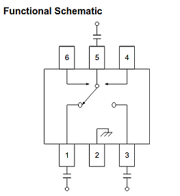
This is the functional diagram from the MACOM data sheet. The switch terminals are obvious and a
pair of control leads (pins 4 and 6)) set the path through the switch. The package is an SOT26
with friendly 0.95 mm lead spacing.
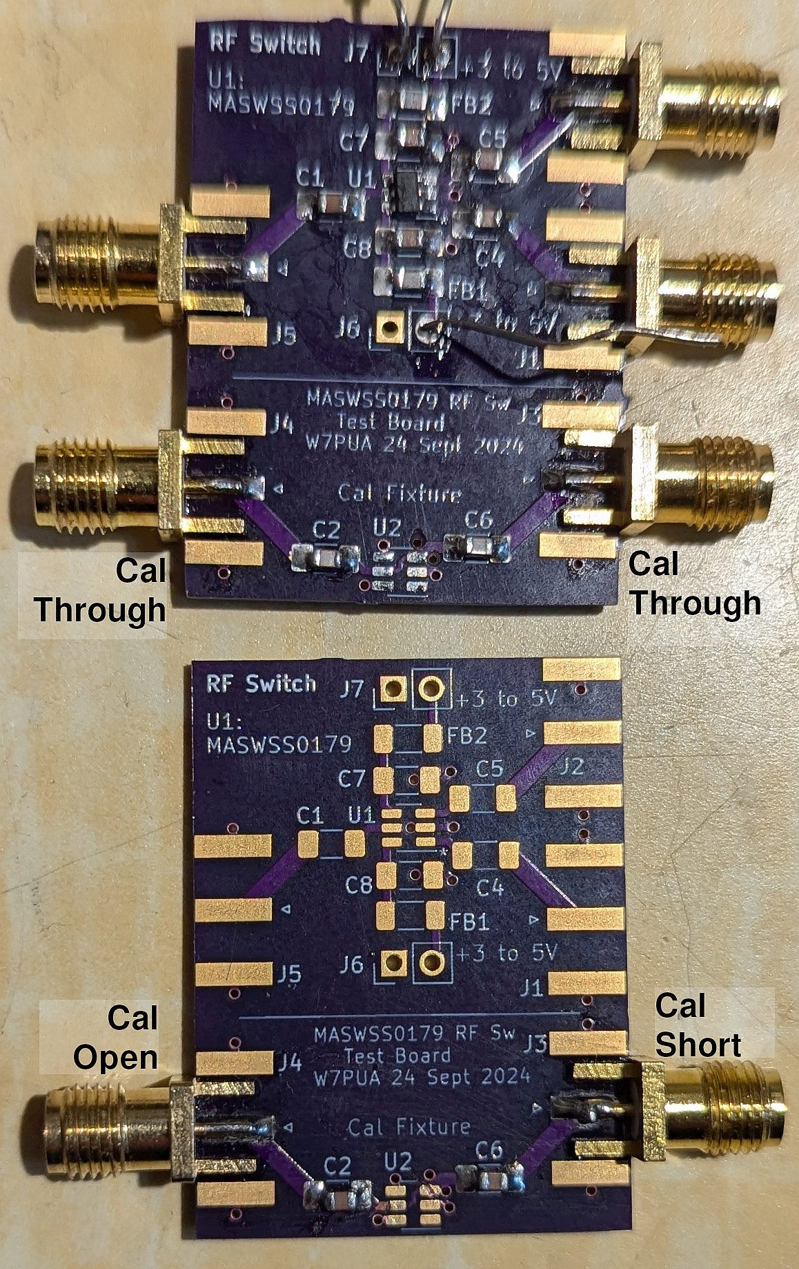
Test Fixture - This board was used to evaluate the RF switches.
The top 2/3 of the board is the working switch with 0.22 uF coupling
capacitors. The bottom part of the board is used for VNA calibration. No
IC is installed in the Cal portion of the board. It provides
a through path by a trace connecting pins 3 and 5. By careful cutting with a
No. 5 Exacto knife, the lower traces also provides an open and a short for reflection
calibration, referenced to the IC pad edges. The SMA edge connectors only have
ground connections on the back of the board. The board thickness is 1.6 mm.
Testing - For frequencies below 60 MHz, evaluation of transmission and reflection was done with
a N2PK VNA. Software was Dave Roberts' "MyVNA." For frequencies up to 3000 MHz, VNA measurements were made with
an HP8714B. The test board included provision for Open, Short and Through calibrations to be made at the IC edge.
This allows the errors related to the PCB to be mathematically removed by the instrument calibration. Thus the
measurements shown are for the IC as an isolated element.
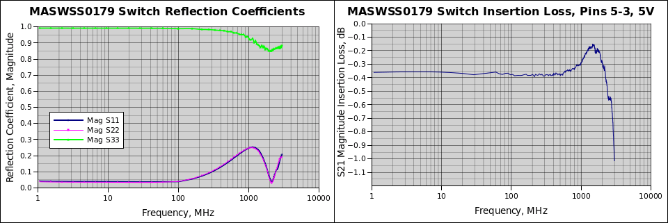
The left graph is the magnitude of the reflection coefficient. This corresponds to the distance
from the center of a Smith chart. Port 1 is the common connection of the switch. Port 2 (IC pin 3) was
always on (+5V to pin 4 and ground to pin 6). Port 3 (IC pin 1) was off, but terminated with 50-Ohms.
The highest reflection coefficient magnitude was about 0.25 about 1200 MHz. This corresponds to a VSWR
of 1.67. The right side graph is the 50-Ohm insertion loss with the Off port terminated. The measured
values shown here seem to be lower than the data sheet values by nore than normal measurement errors. This
suggests that the data sheet includes test PCB losses whereas the data here is for the IC alone.
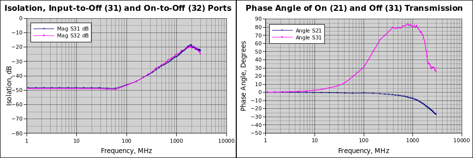
The left graph shows the off isolation. This is both the isolation between the input
port and the Off port (S31) as well as between the On port and the Off port (S32). Not surprisingly,
these differ by only the On insertion loss and some measurement error. The isolation curves agree well with
the data sheet curves. The phase shift curves on the right again do not include the PC board. The 3 GHz
S21 phase shift of 27 degrees is interesting. This would suggest an effective distance, in air, of (27/360)*100 mm
or 7.5 mm. The physical distance between the calibration reference planes is 4 mm, so the rest is due
to slowing of the wave from dielectrics and the IC circuitry.
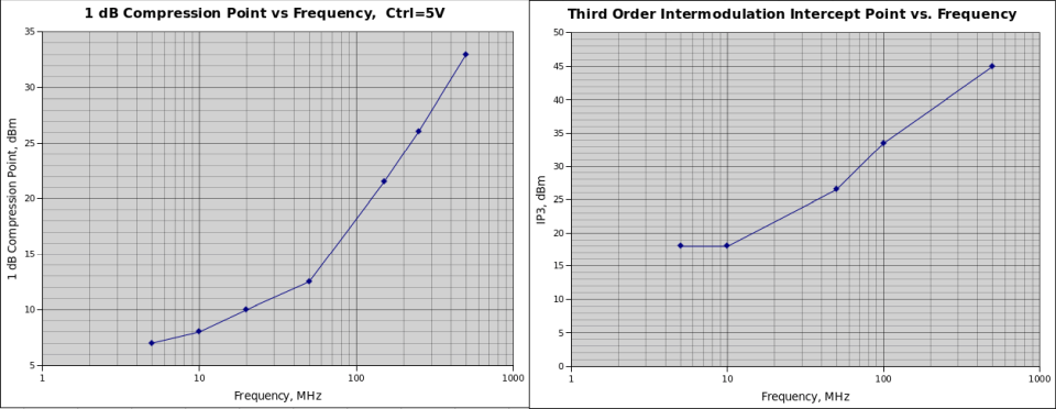
Third-order intermodulation was measured with a pair of Fluke 6060 signal generators, a Janel PD7904 or PD7724 (depending on frequency))
isolated power combiner and a Tek 494AP spectrum analyzer. Measurements were done at 5, 10, 50, 100, and 500 MHz.
The measurement at 500 MHz was at the high limit for my setup, and may be inaccurate. The 50 MHz measurement of 26.5 dBm is
not in agreement with the data sheet (they show +48 dBm typical for +10 dBm signal levels). I re-measured with +5 dBm signal
levels and saw an intercept point of +29 dBm. This appears to be a genuine difference.
The left graph is the 1 dB compression point showing the fast change with frequency. The right graph
shows the related third-order intercept point.
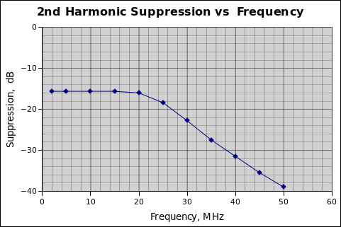
Here is a different take on the lower frequency distortion. In this case the
switch was driven with a single 6060 signal generator at +10 dBm. The output was fed to the spectrun
analyzer where the difference between the desired signal and the 2nd harmonic was measured.
This is a relatively fast test to perform but gives a result that is related to the second
order intermodulation. The range of harmonic power that can be measured is limited by
the second harmonic coming from the signal generator. In this case, that
limits us to 50 MHz or lower. But, it is clear that up to about 20 MHz there is
a consistently high harmonic level coming from the switch, only about 16 dB below the desired 10 dBm signal.
Above 20 MHz, the second harmonic drops off quite rapidly, being down an additional 16 dB at 40 MHz.
Discussion -
At frequencies up through 2 to 3 GHz the MASWSS0179 provides excellent insertion loss, match and isolation.
Above a few hundred MHz, the overload characteristics are outstanding. At lower frequencies, the switch
introduces distortion that can limit the use of the device. At 20 MHz or below the third-order intercept point is
around +18 dBm. That is not nearly as good as the performance at higher frequencies. Yet, for many receiving
applications it may be quite adequate.
It is interesting to compare this GaAs switch with the modern CMOS switches, such as
SN74CBTLV125.
In the 3 to 50 MHZ range, the insertion losses are similar and quite good for both. The isolation for the 179
switch is very good and requires a T arrangement of the 3125 CMOS switches to get close. In this frequency range,
the CMOS single switch has less distortion with an IP3 of 28 dBm versus 18 dBm for the 0179 GaAs switch.
Another comparison is with the miniature mechanical latching relays. Examples of their HF use are
these octave bandwidth filters.
These relays have excellent insertion loss, isolation and distortion numbers in the HF frequency range.
Their downside is the board space and lower levels of reliability. Still, they remain a candidate for low power
RF switching.
Finally, we were asked why the distortion performance drops at lower frequencies. Not having knowledge
of the internal circuitry only leaves us with speculation. But, the distortion performance is consistent with RF
getting into the biasing circuitry, due to some bypass capacitance being inadequate. Maybe someone knows
more about the internal circuitry and can tell us more?