Introduction - This all started while on a backpack in Oregon's Cascade Mountains. We enjoyed the beautiful scenery of our alpine valley. The lake in front of the tent was crystal clear and reflected the surrounding mountains. But, radio signals were all shielded from us. Not only were there no Cell signals, but we could only receive one weak FM broadcast station. The folks back home would really like to know that the bears had not gotten us, but it was not to be (they didn't). I had a 5-Watt 2-meter hand held radio along, but that could not bring up any repeater, even using a half-wave antenna. Then, I remembered being out with Lew, N6QKP, on a similar trip, and he used his Elecraft KX-2 to easily make 75-meter contacts with a simple dipole antenna. This was on SSB and it seemed easy, even in places VHF signals don't get to. The logical conclusion was that I needed one of those.
But logic doesn't always apply. Maybe the KX2 solution was too easy. Maybe it was the challenge of a new design. Certainly, one factor was my familiarity with the Teensy 4.1 and the associated floating point DSP library. But, in any event, I charged off to design and build a radio to meet some fairly specific goals: The original idea was 10 Watts on SSB and CW in a reasonably small package weighing less than 1-pound including a battery. It was to operate on the 80/75 and 40-meter amateur bands and use DSP to the extent possible to enhance both the receiver and transmitters. It was not intended as a home station and would use a small display to both keep things simple and to limit the current draw. The plan was for many hours of receiving time and perhaps 15 minutes of full power transmit time, running off the battery with no charging.
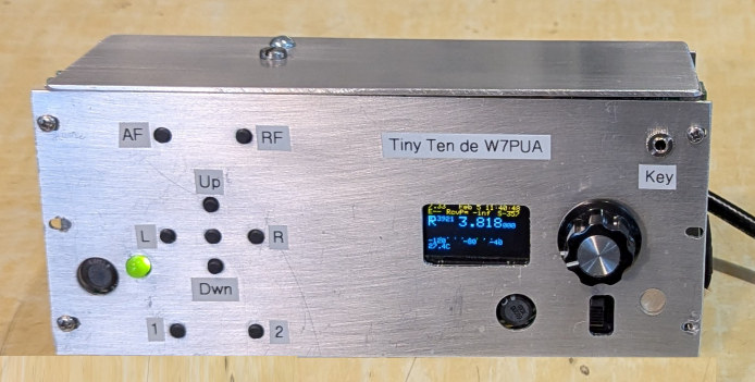
Well, it has been a year and a half since the project started. There were several non-radio distractions, but the radio is now in operation on all modes. The basic goals have been achieved, and as is often the case, the complexity of the radio has grown. This write-up will summarise what the Tiny Ten looks like both physically and functionally. It is not a "how to" writeup, but neither are there any secrets. If you don't see something that interests you, ask, and I'll do my best. However, I have no plans to offer boards or kits.
The radio described by bullet items - This lets you see the general character of the project.
At this time (January 2025) the radio is on the air, but on 80 and 75-meters only. The peak output power is just over 15 Watts. Down below is a list of planned improvements, but for now, it probably needs some use, more than anything. Getting a simple front panel working is one thing; getting the user interface to be easy to use is another thing. On this page, we will try to provide a snap shot of what the radio is, electrically, mechanically and in software.
Electrical Description -

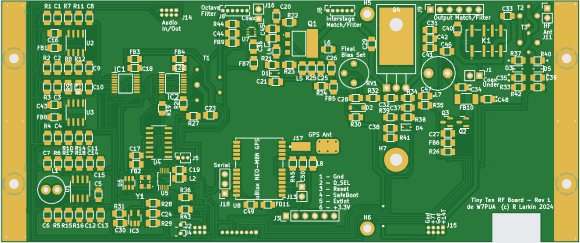
Here is the schematic for the back RF PCB. It includes the LO, the direct conversion I-Q mixer, the RF power amplifier and various switches. This schematic was used in KiCad to generate the images (Gerbers) needed for making the PCB.
Click on the picture to open a readable size in a new browser tab. Close the tab or change tabs to return here.
The hardware architecture is a single RF frequency converter with quadrature signals fed in and out of the DSP. Switches are used at both the RF and I-F level to go between receive and transmit. A single output of the Si5351A synthesizer is used to drive the converter and set the RF frequency. This is run through a 74ALVC74 high speed divide-by-4 to establish precise quadrature conversion signals. This sets the radio's operating frequency. A single RD16HHF MOSFET is the transmit output amplifier. The antenna relay is a latching type to save current. RF filtering and matching networks are on three small PCB; this is an experiment to achieve two objectives. First is to save the weight of multi-band filters, when only one or two bands are actually used. The second objective is to increase the efficiency of the amplifier by using a single-band optimized network rather than broad-band transformers. The two low-level networks are the size of a postage stamp and the output network is about twice that size.

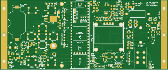
This schematic is the digital PCB. It includes the PJRC Teensy 4.1 processor, the SGTL5000 codec with stereo ADC and DAC, DC voltage conditioning and regulators, the switches, knob and display. This schematic was used in KiCad to generate the images (Gerbers) needed for making the PCB. This PCB mounts in front of the RF PCB by just enough to
Click on the picture to open a readable size in a new browser tab. Close the tab or change tabs to return here.
The digital board centers about the Teensy 4.1 processor. This is a small board that breaks out the multitudes of processor pins as well as providing basic bypassing of power leads and DC power distribution. This both controls the radio and provides floating-point DSP for all receive and transmit signal processing. On the board is an SGTL5000 Codec for audio (I-F) input and output.The digital PCB also has an audio output amplifier that is needed whenhttp://www.janbob.com/electron/TinyTen/TinyTen.htm driving speakers.
Capacitors were a subject of experimentation in this project. Electrolytic and tantalum capacitors have higher series inductance than multi-layer ceramic counterparts, in part because of their larger size. They also have higher series resistance. Finally, they generally have shorter lifetimes (in years) than ceramics. The capacity values available in ceramics have increased as their costs have come down. So this design was done with only ceramic capacitors, with the largest values being 100 microFarads. See this discussion of multi-layer ceramics for more information. In addition, placing multiple values of bypass capacitors in parallel results in undesired parallel resonances (see the referenced link just given and also section 2.8 of Experimental Methods in RF Design). Only identical values were paralleled in this design.
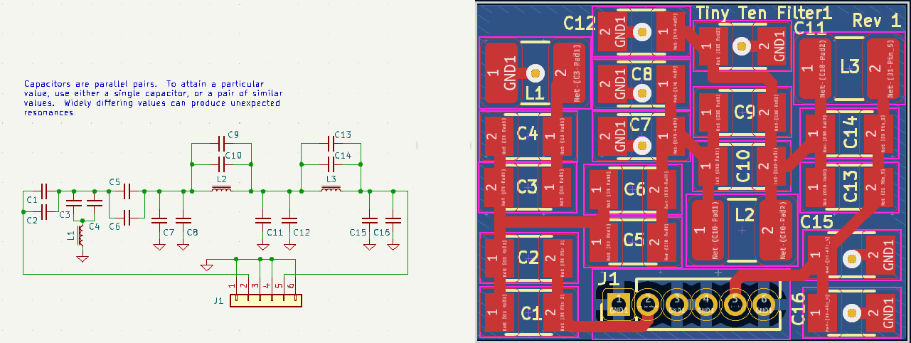
Tuned Circuits - (New writeup as of 31 Jan 2025) For the receive path, the RF filtering consists of octave sized band pass filters. This covers 80 to 10 as 3.5 to 7.3 MHz, 7.3 to 15 MHz and 15 to 30 MHz. This arrangement works fine since the mixers have responses at the 3rd, 5th and other odd harmonics, but not at the even harmonics. The circuits come from previous projects, but instead of using a latching relay, these use a small plug-in card, seen below. The board is quite small, about 0.75-inch (19 mm) across. The header connector has 0.05-inch (1.27 mm) pin spacing
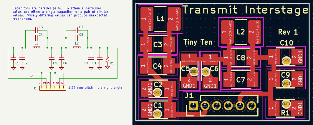
The transmit path uses the same mixer and octave filters as the receiver. This is followed by an 21 dB broadband amplifier and then a plug-in matching network to couple the amplifier to the MOSFET output amplifier. Finally, there is a plug-in matching network to transform the 5 Ohm impedance from the MOSFET to 50 Ohms for the antenna. The 21 dB driver amplifier uses a BFU590 NPN transistor and was designed as a 50 Ohm in-and-out circuit. The plug-in interstage matching network was made quite general in topology as seen next but not all of the components, such as the capacitors shunting the inductors, are used.
Following the transmit path on through, there is the Toshiba RD16HHF MOSFET and a plug-in output network. That network uses a two cascaded L-networks, intended to perfom in the spirit of the wonderful Matthaei transformers (n=4). Since these are plug-in networks, they only cover a single amateur band, providing minimum loss. To allow for best attenuation of harmonics, each inductor can be shunted with a capacitor, placing a notch in transmission at 2nd and 3rd harmonics. In its general form, the output network is shown below. It is a bigger board to allow better current carrying capacity for the connector. The pins are space 0.1-inches (2.54 mm). There is space for T37-6 toroids, as well.
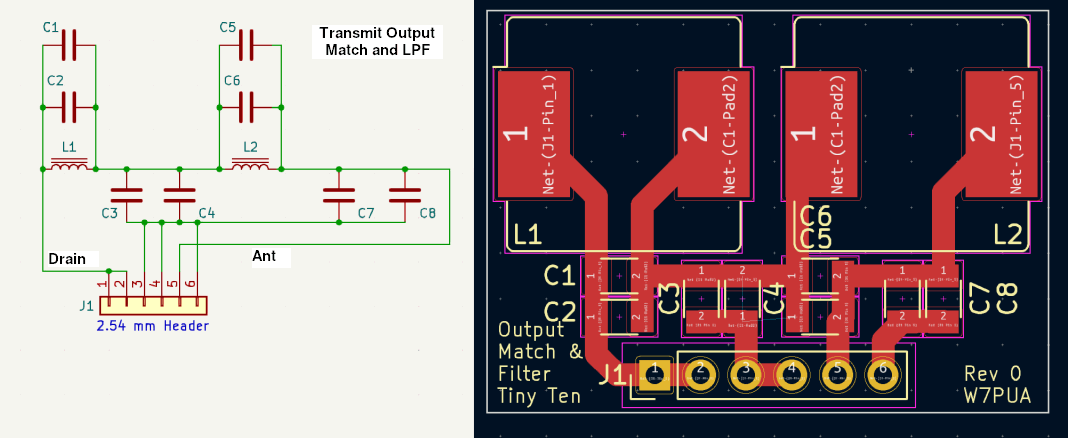
The design approach was to omit the capacitors shunting the inductors and turn the optimizers in ARRL Radio Designer loose on providing 22 dB of gain from the MOSFET amplifier. The Radio Designer script for 10-meters shows an example of this. During optimization, the components for the driver amplifier were fixed as the 21 dB block described above. When implemented on the plug-in boards for 80/75-m, the amplifier performed as expected with output power over 10 Watts. The problem was that the 2nd and 3rd harmonics were only around -20 dB. So it was time to use the notch circuits in the output matching board. Two methods were used for this. They were added to the Radio Designer script with the notch capacitors always constrained to be at the 2nd and 3rd harmonics. This gave fine results, but the approach required setting up the optimization. For existing designs, a simple alternate approach was found to work well.
This method of adding notches at the n-th harmonic, to a design that does not have notch capacitors, involves reducing the inductor value by a factor [1-1/(n^2)] and adding a capacitor of value 1/[(w^2)*L] where w=2*pi*n*fo, fo is the transmit frequency and L is the reduced inductor value. This results in the parallel LC having the same reactance at fo as did the original inductor and a notch at frequency n*fo.
As things will do, the revised output network with notch capacitors did not suppress harmonics as expected. After some measurements and simulation, it was found that sharing of the ground pins on the plug-in connector caused coupling around the network. This is the result of the 20 nH, or so, inductance of the pins. This was cured by slicing the ground plane on the back of the output network board to cause the current in C3 and C4 to flow only through J1-3 and J1-4, while the current in C7 and C8 flowed only through J1-6.
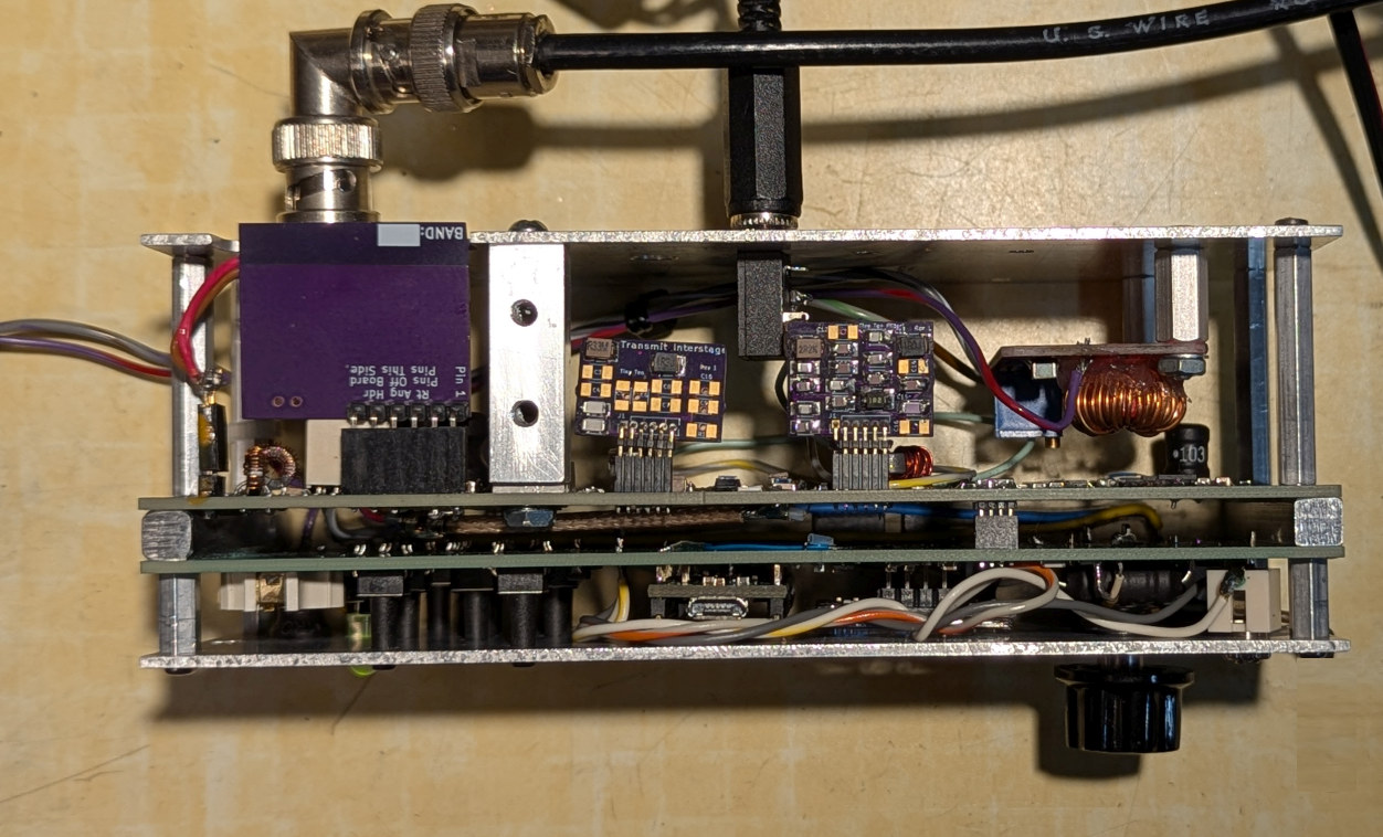
Mechanical Arrangement - Most of the radio is built on two major PCB, the digital and RF PCB's
and a small DC-DC converter. There are also three small plug-in network boards. This is seen in the top photo shown next:
DSP Software - All DSP runs at a fixed 48 kHz sample rate. This supports input frequencies up to about 22 kHz. The receive path uses double conversion principally to increase the flexibility in selection of the Si5351A frequencies to reduce birdies This makes for a first I-F of about 15 kHz. The BFO is then in DSP and essentially birdie free for any required frequency. Phasing method conversions are used at both stages. The transmit path is classic I-Q direct conversion. Using the 15 kHz I-F for transmit can have problems with imperfect carrier suppression leading to opposite side-band re-growth in the following amplifiers. The problem still exists with direct conversion, but it is spectrally hidden by the closeness to the desired side-band. This means that there are more unwanted Si5351A birdies, but they are less of an issue in transmit than in receive.
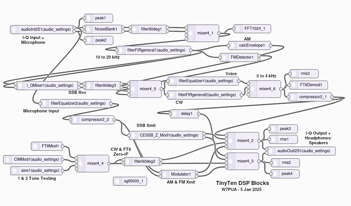
There are various generators, filters and detectors for supporting AM, FM, FT-8, as well as one and two-tone transmitter testing. These functions all come from the floating point DSP library. The following flow diagram is produced by the Design Tool (separate from the 16-bit design tool).
The software is in a single .INO file, plus separate files for some pre-defined FIR filters. It is not currently under any control, but will end up on GitHub, eventually. Here is a copy of the .INO file, as of 15 January 2025. This is not being updated as changes are made, but it gives an idea of the program looks like. Do not attempt to compile this file. I cannot help you at this point in the design process. This file compiled for me and ran the radio, but by the time you read this, I am working on a different un-controlled file. Including quite a bit of working notes, it comes to about 2350 lines, made a bunch smaller by use of the DSP library.
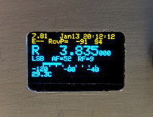
Performance - As of this date, all of the functions are working, except the AM transmit and FT-8 transmit and receive. The AM transmit has the wrong carrier level and the FT-8 is installed in the DSP but has not been tested, yet. Several CW and SSB contacts have been made with good reports. I ran the radio on Straight Key Night and made about 10 contacts. All this was on 80/75, as that is the only transmit output coils I have made. Using no pre-selection, I listened on all bands up to 6-meters. Interestingly, the LO drops out at 208 MHz, stopping the radio before 6-meters stops. I have no intention of trying to make things work at 6-meters and operation at 10-meters is reliable. The sensitivity of the receiver drops off at the higher bands apparently because the LO introduces noise (not phase noise). This needs further exploration. Power output at 3.8 MHz is limited by the RF amplifier to 16 Watts. Ten Watts was the goal and it will be interesting to see how this holds up as we go up in frequency.
The CESSB works well. Signals sound good on SSB. FM seems to work fine, but I didn't spend much time on it. Opposite side-band suppression on transmit is 43 dB (single 1 kHz tone). Carrier suppression is higher. This is without any amplitude/phase corrections. There are corrections available if needed for the higher bands.
The TCXO calibration procedure has been worked out, starting with putting the radio in the freezer. The various checks at 80/75 meters have shown the frequency to be within 1 Hz. It may not always be that good! The real-time clock works fine, and I have so far worked with the ability of the Teensy/Arduino loader to set the clock. The 2032 battery backup has worked fine.
Performance, I-Q Balance - [Added 16 Feb 2025] I measured the phase and amplitude balance for reception by introducing an RF signal of -50 dBm at the antenna connector coming from a Fluke 6060B synthesized signal generator. In software, a DSP phase detector from the Teensy F32 library, AudioAnalyzePhase_F32, was placed at the ADC inputs corresponding to I and Q inputs. Peak detectors were already in place, so we had accurate measurement of the analog I and Q vector voltages. These voltages are important as they are combined through phase shift networks to produce I-F signals in the 15 kHz range. If I and Q are not equal in amplitude and 90 degrees separated in phase, an image signal will be received when tuned 30 kHz below the desired one. See KK7B's detailed discussion and analysis of this in Section 9.2 of Experimental Methods in RF Design. Note that the measurements shown here are without any corrections. Two term corrections could be applied to cancel the errors. The following graph shows the measured I-Q phase shift.
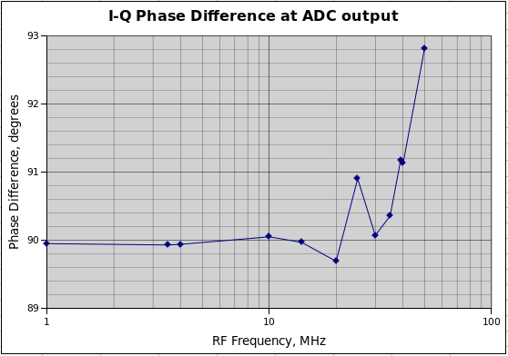
Throughout the frequency range, the amplitude match of I and Q was typically a ratio 1.004, corresponding to image rejection of 48 dB. In constructing the RF board I had the luxury of many 1% resistors and matched these up as best I could. Even the four Tayloe pulse storage capacitors were matched. This all shows up in the tight amplitude control of I and Q. Regardless, if I-Q amplitude correction was applied in the DSP, the resistor matching would be unnecessary.
I measured the image rejection at a few RF frequencies. The measured values are consistent with the values calculated by the KK7B formulas, referenced above. Here are a couple of measurements with 14 MHz representing the lower frequency numbers and 39 MHz corresponding to a frequency with higher phase errors.
14 MHz  |I|/|Q|=1.0035,  dPhase=89.97 deg, Image=-48 dB (calculated -49 dB)
39 MHz  |I|/|Q|=1.0091,  dPhase=91.17 deg, Image=-37 dB (calculated -34 dB)
In general, the plan for now is to proceed without using corrections, possibly adding them in later. One further comment is that somehow I managed to get this far, forgetting to put in Twin Peaks restarts for the SGTL5000 Codec. This was needed, of course, and has been added to the hardware and INO using the AlignLR DSP library class.
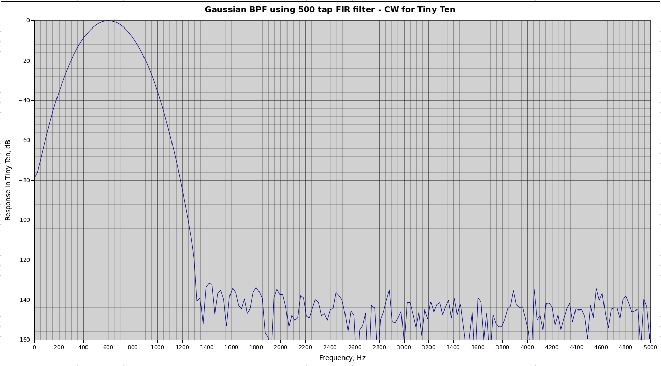
Performance, Audio Filters
Planned Enhancements -
TBD! But this will include getting FT-8 working for sending and receiving 13-character messages on non-standard FT-8 frequencies, finishing the front panel, testing on 10 and 20-meters. Probably a temperature overload sensor will be added to RF transmit output. The front panel needs marking. Plus more.
Thank you -
There are a lot of people who have contributed over the years to I-Q conversion technology for receiving and transmitting. Thanks to all of those. Also, K7MDL, KK7B, W7ZOI, K3KHF, W7GLF, VU2ESE, DD4WH, N6QKP, W7CQ, KF5N, AC8GY & W8TEE along with others on the T41 transceiver project, Paul Stoffregen and his associates with the Teensy processors, and Chip Audette all shared invaluable information. I did not look inside the Elecraft KX2 until after this radio was on the air, but just having seen it and used KK7P's fine software had its influence. Special thanks to KJ7ERE and KJ7EFX for patience and inspiration! Bob, W7PUAIssued 15 January, 2025. Last Revised: - All Copyright © Robert Larkin 2025