Introduction - Without attempting to cover the history of ladder crystal filters, the references at the end of Chapter 3 of Experimental Methods in RF Design are a good start. For this particular experimental filter, I started from the 27 MHz filter designed by Farhan VU2ESE - see "sBITX – An open source SDR that you can hack" at 2021 Four Days in May (FDIM) QRP conference. The goal was to explore the use of miniature ECS fundamental 32 MHz crystals in filters.
The application of this filter is as described by Farhan for transmit and receive with DSP low I-F. That works with transceivers using a conversion to/from 32 MHz with fairly large LO steps of perhaps 5 kHz. Fine tuning is then done in DSP at a second I-F of perhaps 20 kHz. The wide bandwidth of this crystal filter supports having a spectral display showing off-frequency signals as well as allowing wider band modes. This bandwidth of about 35 kHz needs to fit into the half-sample rate of the following ADC. Thus, a sample rate of 96 kHz would work well with this filter.
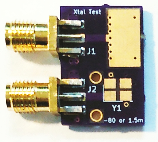
Design process - The first step is to characterize the crystals, in this case ECS-320-12-33B-CKY-TR available from Mouser, Digi-Key and others. A test fixture was laid out on a PCB (see the photo above and XtalTest shared project at OSH Park.) This allowed OSL calibration of VNA measurements referenced to the crystal pad, with O and L coming from the J2 crystal measurement port and S from the shorted J1. The following crystal parameters resulted:
  fs = 31993.8 kHz
  fp = 32050.0 kHz
  Rs = 13.8 Ohms
  Cp = 1.3 pF measured at 30 MHz

These translate to
  Cs = 0.004204464026 pF
  Ls = 5.8856243714 mH
  Qu = 85700
Multiple measurements with the test fixture showed this result to be typical of the batch, all of which are quite similar..
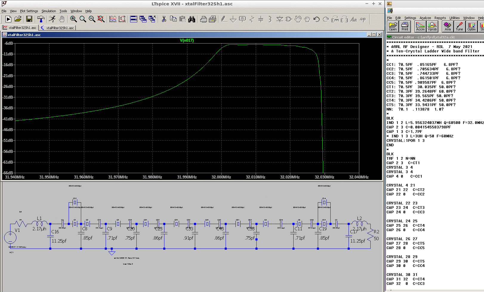
Step 2 was to make a computer model using ARRL RF Designer (ARD). The topology was a symmetrical tuned crystal ladder using double crystals on the ends. This was setup to optimize S11 Input return loss match across a 30 kHz wide passband. For reasons not understood, ARD was not calculating reasonable S21 values, even though S11 and S22 were as expected. I have not seen this before, but it was confirmed by entering all the values into LTSpice. Also, it might be noted that Farhan's use of the double crystals on the input and output was validated in the simulation. I explored carrying this further into the filter but it was not helpful. The following graph summarizes the resulting design (the ARD values are on the far right side of the gif).
High Q is needed for the inductors in the L-network impedance matching. Some 1.8uH SMD inductors show Q's in the 20 or 30 range. This results in high insertion loss and poor S11 and S22. The inductors used were ceramic core wound 1812 Coilcraft parts, 1812CS-182XJLC. These provide a Q of about 75 at 32 MHz, which will be seen to be adequate.
Step 3 is to create a layout for a PC Board. The intention was to make this an SMA connected 50-Ohm building block. A look at the schematic showed capacitances less than 1pF which suggested the need for limiting stray capacitance. The general plan was to use a double sided board with no traces under the crystals or chip capacitors. Substantial ground paths would go down the length of the board to reduce ground loop issues and also allow tin-plate shields, if needed. The board is at OSH Park shared boards as XtalFilter1 https://oshpark.com/shared_projects/NhRWeJmq.
The crystals are very small and have no side metal except at two corners.The pads for the corners need to extend from the crystals far enough for access by a small soldering iron.
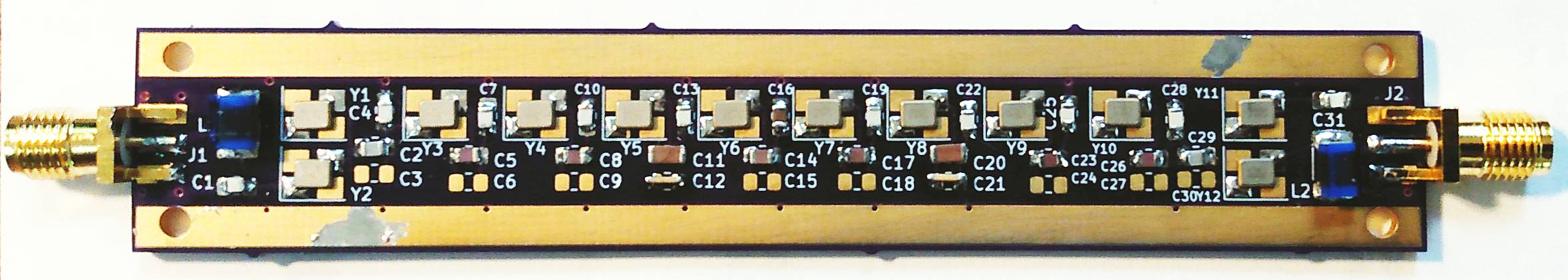
This photo shows the small crystals, along with the 0805 capacitors and two 1812 inductors. The board is double sided, and there are exposed ground strips top and bottom on both sides. The area under the crystals is not filled with ground in order to minimize the stray capacity to ground. SMA connectors are used for the 50-Ohm input and output. Using the part designations seen on the PC board, the capacitor values use were C1=C31=12pF, C2=C29=30pF, C5=C8=C23=C26=39pF, C11=C20=30pF, C12=C21=4.7pF, C14=C17=33Pf, C4=C7=C10=C13=C19=C22=C25=C28=0.7pF, C16=1.0pF.
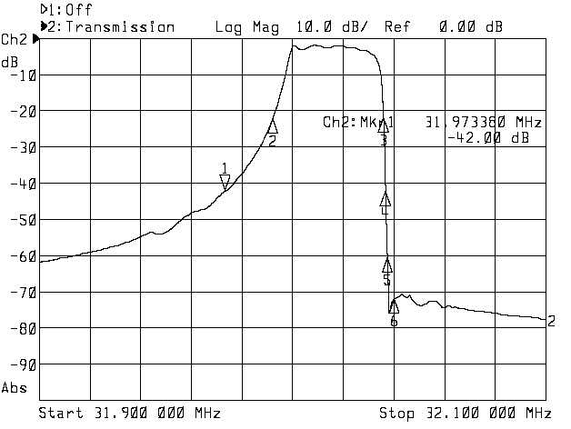
And the response measured on the HP8714B is shown in the next 3 graphs.
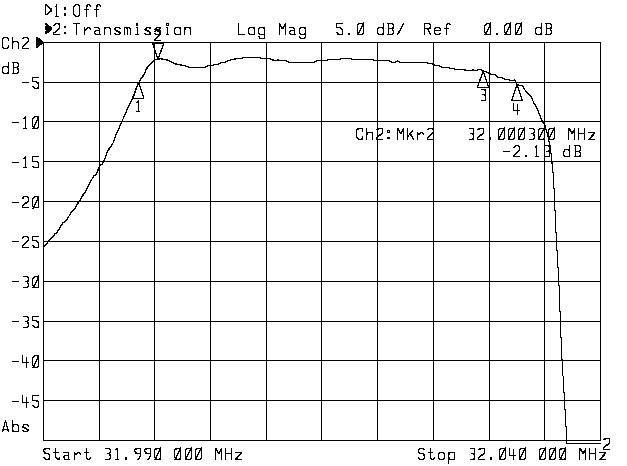
The graph above shows the details of the pass band. The rolloff on the high frequency side is characteristic of these type of ladder filters and is related to the higher frequenciy zeros and the finite Q of the crystals.
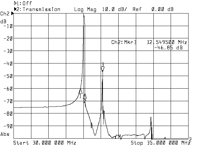
The graph above shows that there are "trapped energy" responses above the pass band. These are far enough away (around 500 kHz)) to not be an issue for either transmit nor for receive.
Improvements and Changes - The crystal has 4 pads. Only 2 of these connect to the crystal. I ended up not soldering to the two "ground" pads and the result is an uncertain connection. This all resulted from concern about bad effects of stray capacities as the impedance of the filter is quite high. The next board revision will omit the two ground pads on the PCB, which should be satisfactory as it minimizes stray capacities and is certain as to connections.
No effort was made to experimentally optimize the L-network impedance matching.. The ripple is a bit more in the measured response than was predicted from the simulation. It might be that some improvement could come from adjustments to the matching.
Issued 11 August 2021. - All Copyright © Robert Larkin 2021