Introduction - This all started while on a backpack in Oregon's Cascade Mountains. We enjoyed the beautiful scenery of our alpine valley. The lake in front of the tent was crystal clear and reflected the surrounding mountains. But, radio signals were all shielded from us. Not only were there no Cell signals, but we could only receive one weak FM broadcast station. The folks back home would really like to know that the bears had not gotten us, but it was not to be (they didn't). I had a 5-Watt 2-meter hand held radio along, but that could not bring up any repeater, even using a half-wave antenna. Then, I remembered being out with Lew, N6QKP, on a similar trip, and he used his Elecraft KX-2 to easily make 75-meter contacts with a simple dipole antenna. This was on SSB and it seemed easy, even in places VHF signals don't get to. The logical conclusion was that I needed one of those.
But logic doesn't always apply. Maybe the KX2 solution was too easy. Maybe it was the challenge of a new design. Certainly, one factor was my familiarity with the Teensy 4.1 and the associated floating point DSP library. But, in any event, I charged off to design and build a radio to meet some fairly specific goals: The original idea was 10 Watts on SSB and CW in a reasonably small package weighing less than 1-pound including a battery. It was to operate on the 80/75 and 40-meter amateur bands and use DSP to the extent possible to enhance both the receiver and transmitters. It was not intended as a home station and would use a small display to both keep things simple and to limit the current draw. The plan was for many hours of receiving time and perhaps 15 minutes of full power transmit time, running off the battery with no charging.
Well, it has been a year and a half since the project started. There were several non-radio distractions, but the radio is now in operation on all modes. The basic goals have been achieved, and as is often the case, the complexity of the radio has grown. This write-up will summarize what the Tiny Ten looks like both physically and functionally. It is not a "how to" writeup, but neither are there any secrets. If you don't see something that interests you, ask, and I'll do my best. However, I have no plans to offer boards or kits.
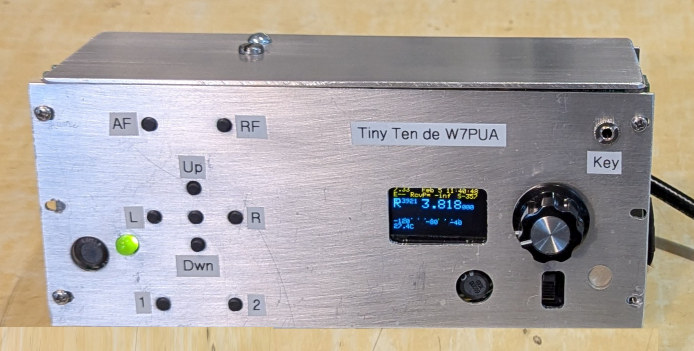
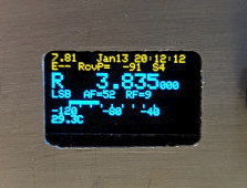
A couple of words on what this radio is and what it isn't. I wanted a real radio in the sense that the receiver sensitivity, dynamic range and selectivity would not limit the ability to communicate. The transmitter needed to be able to generate clean signals and provide enough power output to communicate on CW and FT8 any time and SSB most of the time. The use of CESSB produces clean signals with the effectiveness of a 25 Watt conventional SSB transmitter. The frequency accuracy and stability needed to be right on, with no question as to where we were in the band. In addition, the weight and size needed to be back packable by an old guy. The choice of displays gets down to the second purpose for the rig, that being an opportunity to test out various ideas, such as small displays. The main reasons for the small display was low power consumption. But, it is also an opportunity to experiment with ways to make the most of a minimalist control interface. I already knew what could be done with 50 knobs and switches along with a 10-inch display. It is time to see what can be done with 8 lines of 21 characters plus graphics!
And the architecture. I am a big fan of using double analog conversion with a "wide-band" crystal filter at the first I-F. This allows big steps, like 5 kHz, on the 1st LO which can be essentially birdie free. It provides a lot of protection from interfering signals, as the crystal filter can be early in the gain progression. And finally this gives great flexibility for clean transmitter signal generation. Examples of this approach are the DSP-10 2-meter transceiver and VU2ESE's sBitx HF transceiver (search on either). But, the Tiny Ten does not follow that path, but uses the currently popular path of single conversion to DSP frequencies. This is simpler to build and probably for a lower power portable radio is quite adequate in performance. It also gives me a chance to play with this architecture that I had not done before. I hope to say more about the testing and design of this radio, as time allows.
The radio described by bullet items - This lets you see the general character of the project.
At this time (January 2025) the radio is on the air, but on 80 and 75-meters only. The peak output power is just over 15 Watts. Down below is a list of planned improvements, but for now, it probably needs some use, more than anything. Getting a simple front panel working is one thing; getting the user interface to be easy to use is another thing. On this page, we will try to provide a snap shot of what the radio is, electrically, mechanically and in software.
Electrical Description -
 22 Feb 2025. The Twin Peaks circuitry is the biggest addition.

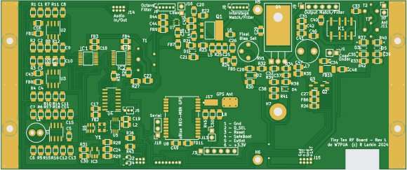
Here is the schematic for the back RF PCB. It includes the LO, the direct conversion I-Q mixer, the RF power amplifier and various switches. This schematic was used in KiCad to generate the images (Gerbers) needed for making the PCB.
Click on the picture to open a readable size in a new browser tab. Close the tab or change tabs to return here.
Not shown here is the circuitry for a GPS module to lock the transceiver frequency and provide time and grid squares. The pads are on the RF board, but it has not been populated nor tested.
The hardware architecture is a single RF frequency converter with quadrature signals fed in and out of the DSP. Switches are used at both the RF and I-F level to go between receive and transmit. A single output of the Si5351A synthesizer is used to drive the converter and set the RF frequency. This is run through a 74ALVC74 high speed divide-by-4 to establish precise quadrature conversion signals. This sets the radio's operating frequency. A single RD16HHF MOSFET is the transmit output amplifier. The antenna relay is a latching type to save current. RF filtering and matching networks are on three small PCB; this is an experiment to achieve two objectives. First is to save the weight of multi-band filters, when only one or two bands are actually used. The second objective is to increase the efficiency of the amplifier by using a single-band optimized network rather than broad-band transformers. The two low-level networks are the size of a postage stamp and the output network is about twice that size.
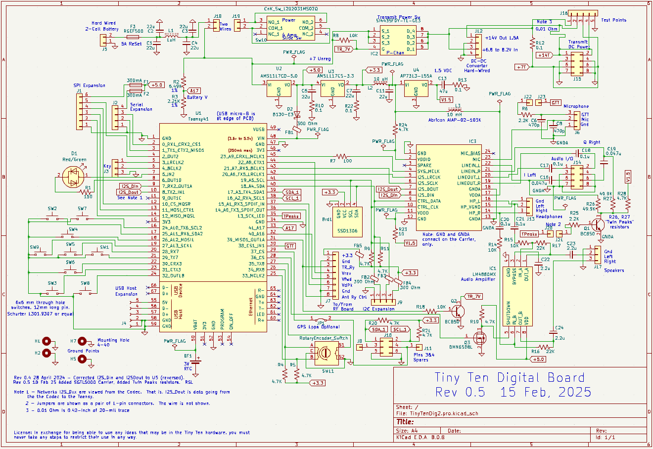
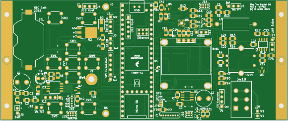
This schematic is the digital PCB. It includes the PJRC Teensy 4.1 processor, the SGTL5000 codec with stereo ADC and DAC, DC voltage conditioning and regulators, the switches, knob and display. This schematic was used in KiCad to generate the images (Gerbers) needed for making the PCB.
Click on the picture to open a readable size in a new browser tab. Close the tab or change tabs to return here.
The digital board centers about the Teensy 4.1 processor. This is a small board that breaks out the multitudes of processor pins as well as providing basic bypassing of power leads and DC power distribution. This both controls the radio and provides floating-point DSP for all receive and transmit signal processing. On the board is an SGTL5000 Codec for audio (I-F) input and output.The digital PCB also has an audio output amplifier that is needed when driving speakers.
Capacitors were a subject of experimentation in this project. Electrolytic and tantalum capacitors have higher series inductance than multi-layer ceramic counterparts, in part because of their larger size. They also have higher series resistance. Finally, they generally have shorter lifetimes (in years) than ceramics. The capacity values available in ceramics have increased as their costs have come down. So this design was done with only ceramic capacitors, with the largest values being 100 microFarads. See this discussion of multi-layer ceramics for more information. In addition, placing multiple values of bypass capacitors in parallel results in undesired parallel resonances (see the referenced link just given and also section 2.8 of Experimental Methods in RF Design). Only identical values were paralleled in this design.
Tuned Circuits - (New write-up as of 31 Jan 2025) For the receive path, the RF filtering consists of octave sized band pass filters. This covers 80 to 10 as 3.5 to 7.3 MHz, 7.3 to 15 MHz and 15 to 30 MHz. This arrangement works fine since the mixers have responses at the 3rd, 5th and other odd harmonics, but not at the even harmonics. The circuits come from previous projects, but instead of using a latching relay, these use a small plug-in card, seen below. The board is quite small, about 0.75-inch (19 mm) across. The header connector has 0.05-inch (1.27 mm) pin spacing
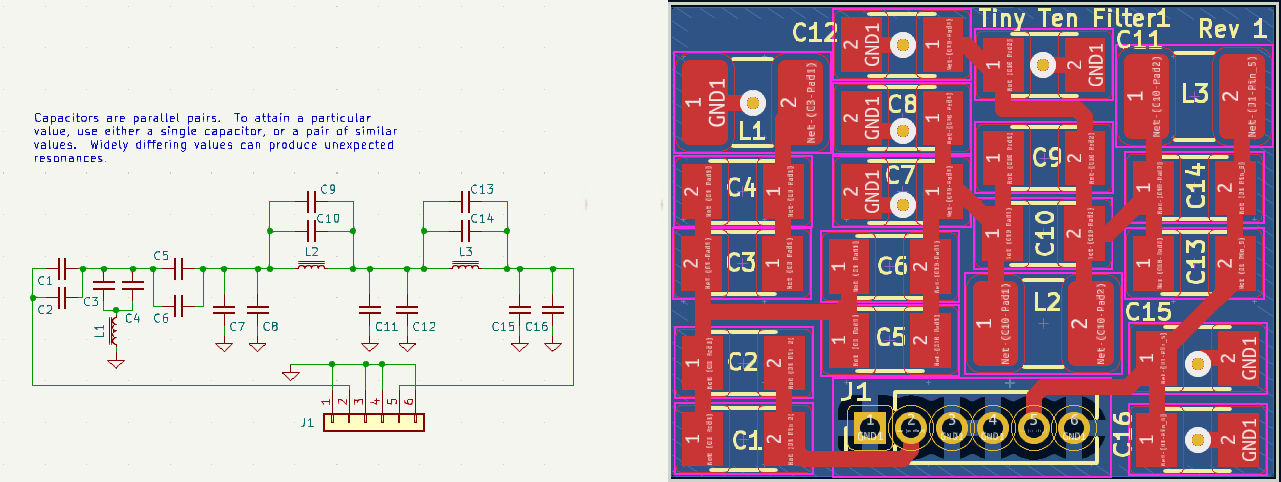
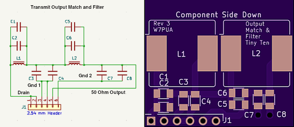
The transmit path uses the same mixer and octave filters as the receiver. This is followed by an 21 dB broadband amplifier and then a plug-in matching network to couple the amplifier to the MOSFET output amplifier. Finally, there is a plug-in matching network to transform the 5 Ohm impedance from the MOSFET to 50 Ohms for the antenna. The 21 dB driver amplifier uses a BFU590 NPN transistor and was designed as a 50 Ohm in-and-out circuit. The plug-in inter-stage matching network was made quite general in topology as seen next but not all of the components, such as the capacitors shunting the inductors, are used.
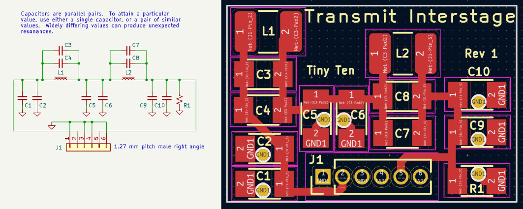
Following the transmit path on through, there is the Toshiba RD16HHF MOSFET and a plug-in output network. That network uses a two cascaded L-networks, intended to perform in the spirit of the wonderful Matthaei transformers (n=4). Since these are plug-in networks, they only cover a single amateur band, providing minimum loss. To allow for best attenuation of harmonics, each inductor can be shunted with a capacitor, placing a notch in transmission at 2nd and 3rd harmonics. In its general form, the output network is shown below. It is a bigger board to allow better current carrying capacity for the connector. The pins are space 0.1-inches (2.54 mm). There is space for T37-6 toroids, as well.
The design approach was to omit the capacitors shunting the inductors and turn the optimizers in ARRL Radio Designer loose on providing 22 dB of gain from the MOSFET amplifier. The Radio Designer script for 10-meters shows an example of this. During optimization, the components for the driver amplifier were fixed as the 21 dB block described above. When implemented on the plug-in boards for 80/75-m, the amplifier performed as expected with output power over 10 Watts. The problem was that the 2nd and 3rd harmonics were only around -20 dB. So it was time to use the notch circuits in the output matching board. Two methods were used for this. They were added to the Radio Designer script with the notch capacitors always constrained to be at the 2nd and 3rd harmonics. This gave fine results, but the approach required setting up the optimization. For existing designs, a simple alternate approach was found to work well.
This method of adding notches at the n-th harmonic, to a design that does not have notch capacitors, involves reducing the inductor value by a factor [1-1/(n^2)] and adding a capacitor of value 1/[(w^2)*L] where w=2*pi*n*fo, fo is the transmit frequency and L is the reduced inductor value. This results in the parallel LC having the same reactance at fo as did the original inductor and a notch at frequency n*fo.
As things will do, the revised output network with notch capacitors did not suppress harmonics as expected. After some measurements and simulation, it was found that sharing of the ground pins on the plug-in connector caused coupling around the network. This is the result of the 20 nH, or so, inductance of the pins. This was cured by slicing the ground plane on the back of the output network board to cause the current in C3 and C4 to flow only through J1-3 and J1-4, while the current in C7 and C8 flowed only through J1-6.
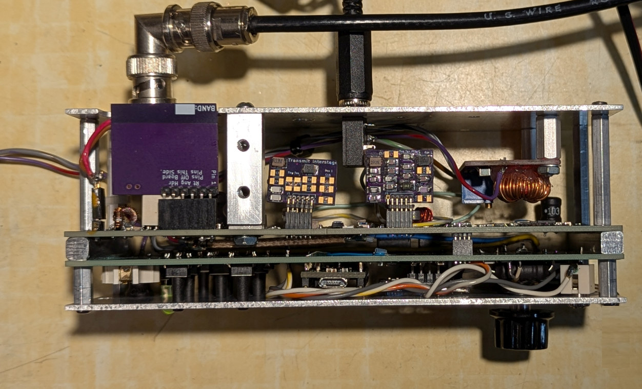
Mechanical Arrangement - Most of the radio is built on two major
PCB, the digital and RF PCB's and a small DC-DC converter. There are also
three small plug-in network boards. This is seen in the top photo shown next:
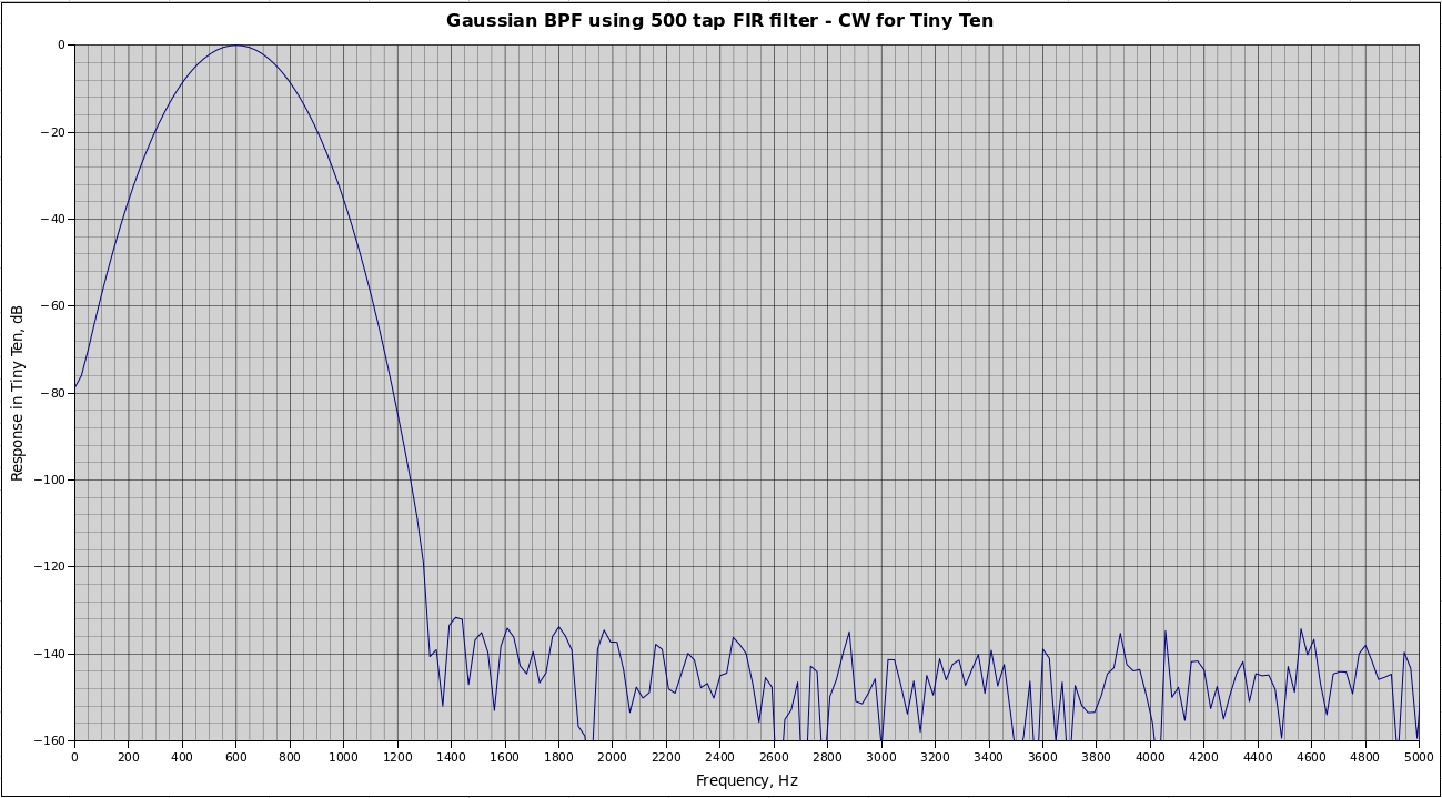
DSP Software - All DSP runs at a fixed 48 kHz sample rate. This supports input frequencies up to about 22 kHz. The receive path uses double conversion principally to increase the flexibility in selection of the Si5351A frequencies to reduce birdies This makes for a first I-F of about 15 kHz. The BFO is then in DSP and essentially birdie free for any required frequency. Phasing method conversions are used at both stages. The transmit path is classic I-Q direct conversion. Using the 15 kHz I-F for transmit can have problems with imperfect carrier suppression leading to opposite side-band re-growth in the following amplifiers. The problem still exists with direct conversion, but it is spectrally hidden by the closeness to the desired side-band. This means that there are more unwanted Si5351A birdies, but they are less of an issue in transmit than in receive.
There are various generators, filters and detectors for supporting AM, FM, FT-8, as well as one and two-tone transmitter testing. These functions all come from the floating point DSP library. The following flow diagram is produced by the Design Tool (separate from the 16-bit design tool).
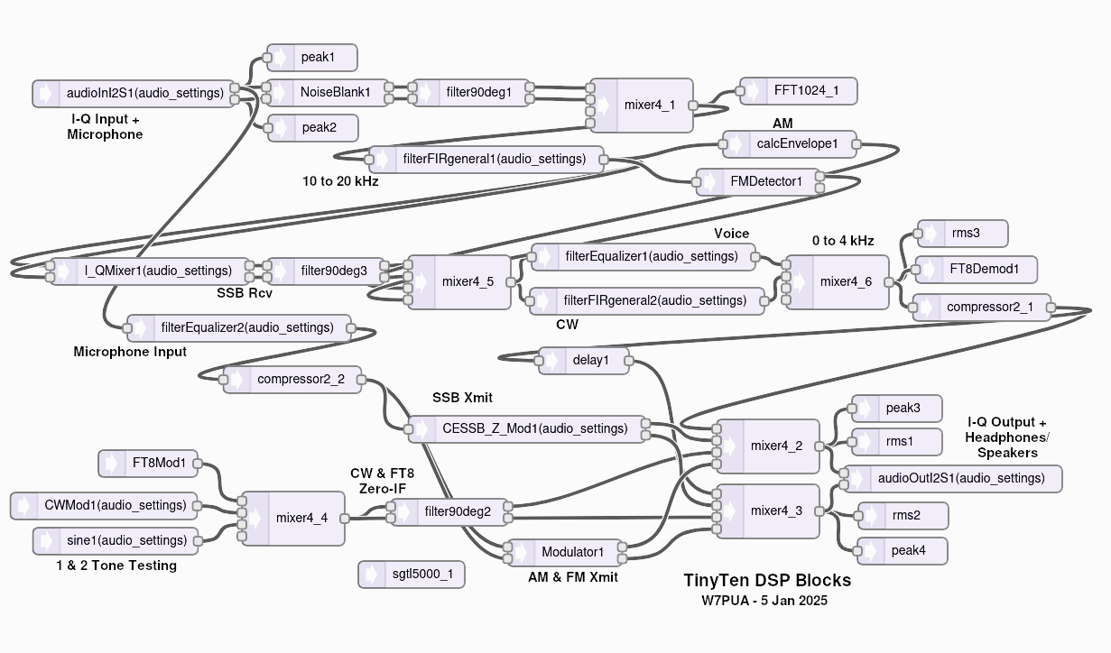 This is the flow diagram created by the Design Tool referenced above. It represents the flow of audio
signals in the Tiny Ten radio. What is less obvious is that within the DSP software, the
lines between blocks will create "connecting"
objects that work with the audio streaming system to ensure that the audio data are transferred as needed.
This all happens automatically once the blocks and connections are instantiated. It makes it simple system
to design and program the audio/I-F processing. Note that this diagram is not up-to-date in that there is
a block, not shown, for the AudioAlign_F32 library class that corrects a problem in the SGTL5000 ADC
that randomly mis-aligns the I and Q channels by one sample. This sits between the audioInI2S1 and NoiseBlank1.
This is the flow diagram created by the Design Tool referenced above. It represents the flow of audio
signals in the Tiny Ten radio. What is less obvious is that within the DSP software, the
lines between blocks will create "connecting"
objects that work with the audio streaming system to ensure that the audio data are transferred as needed.
This all happens automatically once the blocks and connections are instantiated. It makes it simple system
to design and program the audio/I-F processing. Note that this diagram is not up-to-date in that there is
a block, not shown, for the AudioAlign_F32 library class that corrects a problem in the SGTL5000 ADC
that randomly mis-aligns the I and Q channels by one sample. This sits between the audioInI2S1 and NoiseBlank1.
The software is in a single .INO file, plus separate files for some pre-defined FIR filters. It is not currently under any control, but will end up on GitHub, eventually. Here is a copy of the .INO file, as of 21 February 2025. This is not being updated as changes are made, but it gives an idea of the program looks like. Do not attempt to compile this file. I cannot help you at this point in the design process. This file compiled for me and ran the radio, but by the time you read this, I am working on a different un-controlled file. Including quite a bit of working notes, it comes to about 2500 lines, made a bunch smaller by use of the DSP library.
Performance - As of this date, all of the functions are working, except the AM transmit and FT-8 transmit and receive. The AM transmit has the wrong carrier level and the FT-8 is installed in the DSP but has not been tested, yet. Several CW and SSB contacts have been made with good reports. I ran the radio on Straight Key Night and made about 10 contacts. All this was on 80/75, as that is the only transmit output coils I have made. Using no pre-selection, I listened on all bands up to 6-meters. Interestingly, the LO drops out at 208 MHz, stopping the radio before 6-meters stops. I have no intention of trying to make things work at 6-meters and operation at 10-meters is reliable. The sensitivity of the receiver drops off at the higher bands apparently because the LO introduces noise (not phase noise). This needs further exploration. Power output at 3.8 MHz is limited by the RF power amplifier to 16 Watts. Ten Watts was the goal and as of this writing (22 Feb 25) the coil boards have been built for 10-meters and 12 Watts of power output has been measured. This needs further measurements before saying that 10-meters is ready.
The CESSB works well. Signals sound good on SSB. FM seems to work fine, but I didn't spend much time on it. Opposite side-band suppression on transmit is 43 dB (single 1 kHz tone). Carrier suppression is higher. This is without any amplitude/phase corrections. There are corrections available if needed for the higher bands.
The TCXO calibration procedure has been worked out, starting with putting the radio in the freezer. The various checks at 80/75 meters have shown the frequency to be within 1 Hz. It may not always be that good! The real-time clock works fine, and I have so far worked with the ability of the Teensy/Arduino loader to set the clock. The 2032 battery backup has worked fine.
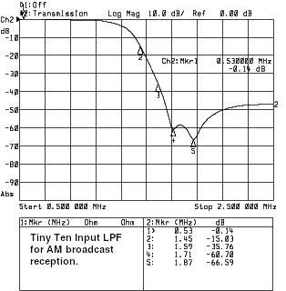
North American AM Broadcast Band - This is a bonus band. I made up a modified octave filter to cover 530 to 1400 kHz, in part to see how well it works and in part to be able to listen to the AM band. In order to not have a station at 1590 kHz appear at 1590/3=530 kHz, the filter was designed to have a cutoff at almost 1400 kHz. This gives up the top 300 kHz of the band. A Dremel tool was used to convert the use of L1 from a HP to a LP filter, but not using any notch with it. The other two transmission poles were built, as usual, from L2 and L3 and associated capacitors. These two had capacitors to add notches. The component values are shown along with the graph of transmission. In general, this design is limited by the 1812 chip inductor Qu. Always a compromise. As far as performance, the sensitivity is very good, x3 frequency stations have not shown up, and the quality of the sound from the DSP envelope detector is very good. I like the synthesized stereo sound from the delay binaural.
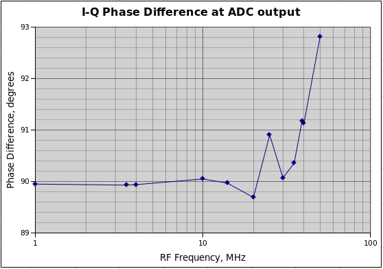
Throughout the frequency range, the amplitude match of I and Q was typically a ratio 1.004, corresponding to image rejection of 48 dB. In constructing the RF board I had the luxury of many 1% resistors and matched these up as best I could. Even the four Tayloe pulse storage capacitors were matched. This all shows up in the tight amplitude control of I and Q. Regardless, if I-Q amplitude correction was applied in the DSP, the resistor matching would be unnecessary.
I measured the image rejection at a few RF frequencies. The measured values are consistent with the values calculated by the KK7B formulas, referenced above. Here are a couple of measurements with 14 MHz representing the lower frequency numbers and 39 MHz corresponding to a frequency with higher phase errors.
14 MHz  |I|/|Q|=1.0035,  dPhase=89.97 deg, Image=-48 dB (calculated -49 dB)
39 MHz  |I|/|Q|=1.0091,  dPhase=91.17 deg, Image=-37 dB (calculated -34 dB)
In general, the plan for now is to proceed without using corrections, possibly adding them in later.
Somehow I managed to get this far, forgetting to put in Twin Peaks time shifter for the SGTL5000 Codec. This was needed and has been added to the hardware and INO using the AlignLR DSP library class. At startup, before the LO has been turned on to create a receiver, an i/o pin on the Teensy is used to generate a square wave at about one fourth of the sample rate. This is introduced to both inputs of the ADC. A correlation is made between the I and Q ADC inputs with delays of 0, 1, 2 and 3 sample periods. The positive correlation is found, corresponding to the two channels being aligned. Then this shift is always made to bring the two channels into alignment. This is only required a start-up, as it never shifts while in operation.
Performance, Audio Filters
 Dynamic Range, Noise Figure and Distortion - [Added 5 Mar 2025]
This radio is intended for use in portable locations
where there are not many strong stations. The receiver also does not often need super-sensitivity since
the other end of a QSO is likely using higher power. Never-the-less, the goal is to provide the best
performance that is practical with simple hardware And, in the spirit of experimentation, this radio
gives me an opportunity to learn more about real direct conversion techniques and their performance. So,
we made a series of measurements that resulted in a few changes. Here is a summary
of that activity, and a puzzle about internal noise.
Dynamic Range, Noise Figure and Distortion - [Added 5 Mar 2025]
This radio is intended for use in portable locations
where there are not many strong stations. The receiver also does not often need super-sensitivity since
the other end of a QSO is likely using higher power. Never-the-less, the goal is to provide the best
performance that is practical with simple hardware And, in the spirit of experimentation, this radio
gives me an opportunity to learn more about real direct conversion techniques and their performance. So,
we made a series of measurements that resulted in a few changes. Here is a summary
of that activity, and a puzzle about internal noise.
Basic to measuring overload and sensitivity is to know the gain of the front end, in this case from the antenna input to the CODEC (ADC) output. If this varies large amounts over the frequency range of interest, which in this case is 1.8 to 30 MHz, we need to allow for this. The data, just below, shows that the gain at 30 MHz is only down about 1.2 dB relative to that at 4 MHz. At 30 MHz, the sample pulses for the Tayloe mixer are only 8.3 nSec. If these pulses are effectively reduced in length by the various delays and rise times, this can result in loss in the mixer. This may be a factor in the observed change in loss with frequency, but the good side is that the loss at worst case is only 1.2 dB. The response with frequency is effectively flat.

Let's digress from the measurements to look at a simplified picture of the Tiny Ten receiver.
The next figure, below, is a block diagram of the analog hardware for the receiver. It starts on the
left at the antenna port where we have an antenna relay and other transmitter related hardware,
such as a directional coupler for measuring power and VSWR. The loss through these transmitter
parts is a fraction of a dB and so can be ignored. Next is an "octave" band-pass filter.
This is very important to both the receiver and transmitter as it prevents reception or transmission
at three, and more, times the operating frequency. The mixer that follows is very susceptible to
effects at all odd harmonics. Losses through the filter are generally a dB or less, primarily
because the pass band is not narrow. Following the filter is the
Tayloe switching mixer,
that is also
shown in this application discussion.
An op-amp, set up as a differential amplifier, follows to sum the two mixer outputs and raise the level high enough
for the analog-to-digital converter (ADC). This is then run into the CODEC that starts with a variable
gain amplifier that adds up to 22 dB more gain. Finally the ADC is a sigma-delta type that is inherently very linear.
This ADC is 16 bits, but the lowest 3 or 4 are covered with "noise" that includes some coherent components.

To aid in digging a little deeper into the circuitry, the next schematic shows a portion of the circuitry in the receiver path. The RF transformer, T1, produces two versions of the input signal with equal amplitude and phase separated 180 degrees. This feeds both the in-phase, or "I" switches of the Tayloe mixer as well as the 90-degree or "Q" switches that are not shown since they are the same except for the timing of the sample pulses. The storage capacitors, C1 and C2, are essentially right at the inputs to the op-amp U1. R1 and R2 were included for possible use, but at least for now, the higher gain that comes with making these resistors very small in value, is valuable. At first glance it looks like the gain of op amp is R3/R1 or around 10,000. Not so. As Tayloe points out in the first reference above, the mixer appears to the circuit that follows as a resistance in the order of 200 Ohms, so much less gain is achieved. For our case I determined this resistance by replacing both R1 and R2 with two trial values, 18 Ohms and 100 Ohms and measuring the change in gain. This was measured to be 3.65 dB which, with a bit of arithmetic, showed the equivalent resistance to be 139 Ohms. The resulting simplified circuit is shown on the right. This shows the Voltage gain of the op-amp stage to be 20000/139 = 144, or 43 dB.

Dynamic range is limited by noise on the lower end and by distortion on the upper side. A measure of noise performance is Noise Figure, which tells us how much the radio input circuitry will decrease the signal-to-noise ratio. This definition was used to measure the noise figure at 4 MHz (this is not a great way to measure low noise figures, but, as we will see, ours is not low). A signal at -107 dBm from the Fluke 6060B signal generator was introduced at the antenna terminal. The noise power of this input is that of a resistor at room temperature or -174 dBm/Hz. The resulting noise and signal plus noise were measured in the DSP from which we we found the S/N to be 6.6 dB. The bandwidth of the DSP filter is 10000 Hz giving an input S/N of -107 - (-174 + 40) or 27 dB. Wow, the noise figure is up there at 27 - 6.6 = 20.4 dB. This is way above the expect value in the 6 dB region.
This measurement was repeated at different signal levels with the same answer. The method was applied to other radios. They showed much better noise figures, again suggesting that the high noise figure was not the result of faulty measurements. So, what does this all mean? It is not clear, but a couple of observations may give some hints. I varied the gain of the input amplifier for the ADC over its 22 dB range and the observed noise figure only changed by 0.2 dB, suggesting that the noise from the op-amp dominated over that of the ADC. I also measured curves of noise power with changing receiver frequency. This showed a strong dependency on frequency as seen in the next graph.

Above about 7 MHz, the noise curve above shows a pattern of decreased noise when the radio was wrapped in aluminum foil. This suggests that radiated noise from off the RF board was being picked up. Probing with a few turns of wire as an antenna showed that the 1-inch display was the strongest source of noise on the digital board. The Teensy processor was quite a bit lower in radiation than the display. It was still not clear where the 4 MHz noise was coming from. The lack of improvement with the aluminum foil suggests that conducted noise might be present. The boards have been arranged to have no "always active" digital leads on the RF board. The only digital control leads are an unshared I2C control for the Si5351 and the associated temperature sensor. That I2C is quiet except when the frequency is changed or the temperature is read. These events happen only occasionally. A conducted path does exist out of the Si5351. That needs more investigation.
So, where does this leave us. The higher noise figure is not a problem at all on 80/75 meters, because of strong external noise. That is generally the case on 40-m as well. Going to 30 or 20 meters is a little different deal. Listening on those bands shows many stations being heard. But comparing with other receivers leaves us wanting better. The higher bands like 15-m and 10-m show noise figures in the 25 dB range, or higher, and certainly need better sensitivity. So, how do we get there. More experiments are needed to isolate the source of the noise. If the noise can be brought down, great! Otherwise, the best we can do is to cover up the noise with RF pre-amplification. This is undesired, as the RF gain would be wide-band and eats into the dynamic range in a major way. But it would be very effective in reducing the noise figure.
Let's look at the high-signal-level side of dynamic range. The Tayloe mixer is inherently resistant to overload. The negative feedback of the op-amp circuit makes it quite linear up to the voltage rails where the signal is totally clipped. The same applies to the input amplifier for the ADC. The sigma=delta ADC is likewise highly linear up to the point where all 16-bits are "full". Again the clipping is complete at that point. The Voltage range for the ADC is slightly less than the power rails which means that it will be the point where clipping occurs.
If the radio is driven by a single RF sine wave from the signal generator, there is nothing to observe until the ADC overload occurs and distortion begins. The level for this is about -34 dBm with the ADC input amplifier at minimum gain and about -56 dBm when at maximum. Two tone testing of intermodulation is quite difficult since the sum signals must not overload the ADC placing the intermodulation products, as it turns out, more than 85 dB below the test signals. For my pair of Fluke 6060B generators this puts the IM product into the soup of noise and spurs from the generators. Searching around in the 20 to 50 kHz spacing region, I was able to not see an IM product at -125 dBm from a pair of -40 dBm inputs. This establishes that the receiver front end circuitry was producing a third order input intercept point of at least 2.5 dBm. It was more, but since I couldn't measure it, we don't know how much.
The highly linear input circuitry, along with the sudden clipping of the ADC, is quite a different situation than conventional RF circuitry that has slow gain roll-off. Note that the classic mathematical treatment of intermodulation assume that the polynomial fit of the gain compression has a dominant cubic term. The polynomial fit for sudden clipping has significant coefficients for all odd terms. And, any odd term of the polynomial produces third order distortion, not just the cubic one. If that sounds too complicated, the bottom line is to keep the signal from overloading the ADC and don't worry about the intermodulation.
One last element of the story is birdies generated in the Si5351 synthesizer. That handy signal source uses one or two "fractional-N" synthesizers in order to generate almost abitrary frequencies. This produces a large number of not-too-strong coherent birdy signals. If a birdy hits on the frequency being received it may be the bottom end limitation to sensitivity. It would be interesting to quantify this assertion, but I have not done that. What I did do for the IM testing was to use an LO frequency that had integer division for both synthesizers (specifically 25MHzx27/176 = 3.835227MHz).
Noise Figure of the Mixer Alone - [Added 16 Mar 2025]
As mentioned above, it appeared that the Tiny Ten, running as a full radio was losing sensitivity to digital noise from
some part of the circuit away from the receiver front end. To test this idea, I cut up an RF board to
have the mixer including the divide-by-four LO circuit, but not the Si5351A signal generator. It is shown below.

This was intended to be an "all analog" test and so the LO drive was provided by a Fluke 6060B generator. This seemed to work fine, as the divide-by-four would trigger from sine-wave signals above -3 dBm (or lower). That input was set to +5 dBm. The RF input, if used, was from a separate 6060B. The I-F output was again not sent to an ADC to avoid digital noise possibilities, but rather to an oscilloscope or an Tek 494AP "analog" spectrum analyzer (SA). The latter proved to be the most useful, as it could be tuned to 15 kHz with full performance. The gain of the I-F amplifier was able to override the internal SA noise by about 10 dB (that internal noise was corrected for).
The noise figure was first measured by including a weak sine wave input signal. This method tends
to be inaccurate because, the signal level has been greatly attenuated and also determining the absolute
power of the noise is difficult. The second method is the traditional one used for high accuracy
RF measurements and uses noise sources of two known levels, the Y-Factor test.
I had available an AILTech 7615 noise source and a known
amplifier to check its accuracy. That source is rated down to 10 MHz. So, the procedure
was to measure the noise power with the source both off and on. That gave relative powers. With all units
in milliwatts of power, the previously measures SA input noise power is subtracted from the two measurements.
This is the so-called "second stage correction." Next the Y-Factor is found by dividing the on power by
the off power. Finally, the
the noise figure is calculated and changed to dB, using standard formulas
(equation 20 of the linked reference).
The next figure shows the resulting noise figure as a function of frequency.

The noise figure starts at low frequencies at about 11 dB. The front end filtering loss accounts for about 1 dB of this, there is some small mixer loss which means that an amplifier noise figure around 9 dB would be consistent with the data. That amplifier NF is several dB higher than was expected, but separate amplifier measurements will be deferred for now. The noise figure rises slowly with measurement frequency reaching a value of about 15 dB at 30 MHz. Above 30 MHz, I did not have a band-pass filter available and substituted a jumper wire. This arrangement receives noise at the odd harmonics of the operating frequency that is added to the desired noise powers. This, in turn, makes the noise figure appear lower than it is. Since filtered and jumper-wired measurements were available at 30 MHz, the higher frequency curve was raised by 5.2 dB to make the curves continuous at 30 MHz. The higher curve is shown as a dashed line and should be treated as an estimate.
The gap at 40 MHz is interesting as it reflects the divide-by-four logic failing to operate. I have not explored this beyond observing that it is happening. A 40 MHz receive frequency runs with an input of around 160 MHz that is well within the capability of the 74ALVC logic family that is being used.
Starting around 45 MHz, the noise figure starts to climb and the value of 20 dB at 50 MHz clearly calls for a preamp. Operation ceases completely at about 52 MHz. This all suggests that this is really a 0 to 30 MHz circuit. Higher frequency operation operation may be possible, but performance may also be an issue.
A further set of measurements were done at 10 MHz to study differences in noise figure when the 40 MHz LO source was changed. Three generators were used, a Fluke 6060B, a PTS-160 and a breakout board Si5351A running off an Arduino Uno. There were no measurable differences in either the "On" or "Off" settings of the noise source.
This experiment has shown that the noise figure of the Tiny Ten is not achieving the levels that are possible. It would seem that some sort of RF noise pickup is involved. Up around 30 MHz, this problem is the greatest. Tracking down the ways to fix the issue remains a bit of a puzzle. This will be pursued as time is available.
Planned Enhancements - TBD! But this will include getting FT-8 working for sending and receiving 13-character messages on non-standard FT-8 frequencies, finishing the front panel, testing on 10 and 20-meters. Probably a temperature overload sensor will be added to RF transmit output. The front panel needs marking. Plus more.
Thank you -
There are a lot of people who have contributed over the years to I-Q conversion technology for receiving and transmitting. Thanks to all of those. Also, K7MDL, KK7B, W7ZOI, K3KHF, W7GLF, VU2ESE, DD4WH, N6QKP, W7CQ, KF5N, AC8GY & W8TEE along with others on the T41 transceiver project, Paul Stoffregen and his associates with the Teensy processors, and Chip Audette all shared invaluable information. I did not look inside the Elecraft KX2 until after this radio was on the air, but just having seen it and used KK7P's fine software had its influence. Special thanks to KJ7ERE and KJ7EFX for patience and inspiration! Bob, W7PUAIssued 15 January, 2025. Last Revised: 22 Feb 2025 - All Copyright © Robert Larkin 2025. Hardware license: In exchange for being able to use any ideas that may be in the Tiny Ten hardware, you must never take any steps to restrict their use.